Last updated on 1 June 2024 by Suffocation
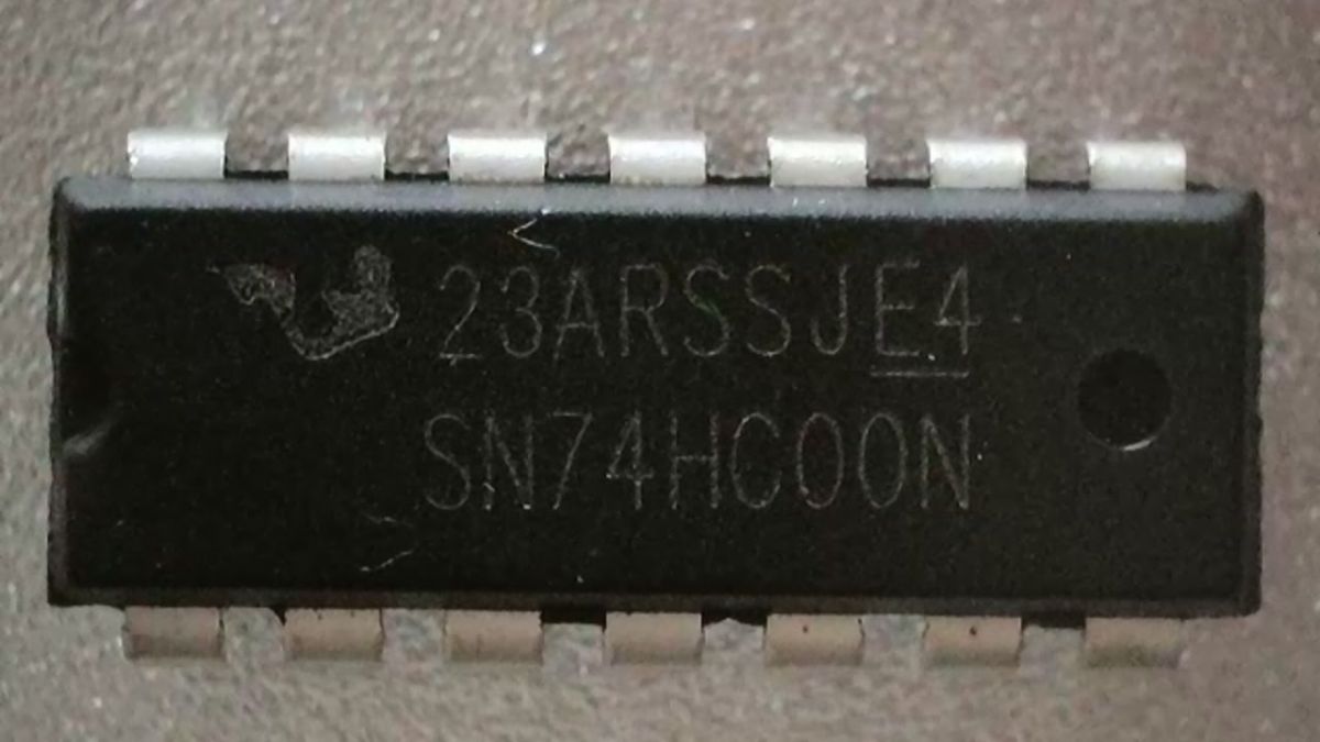
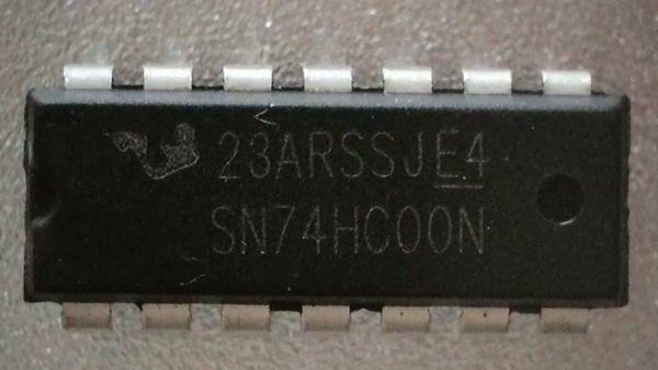
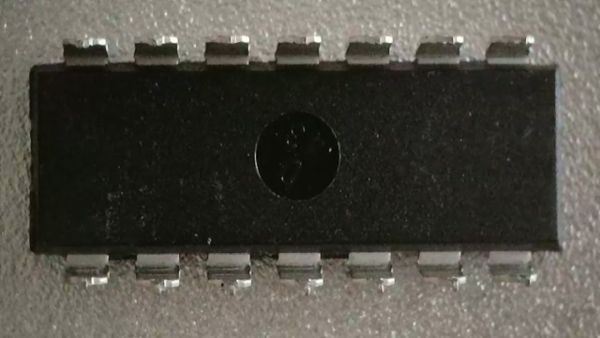
Four NAND gates in one IC. With the first IC of the TTL series, further basic circuits can be created, so that only one type of IC would be needed. This made the IC so versatile and popular in its time. Unfortunately, the era of TTL components is over; today, these are mostly replaced by small controllers that can map complex logic by being programmed with software. Nevertheless, this component also marks the beginning of my TTL series. The use of these components serves to improve basic understanding, which is helpful as a basis for more complex circuits or also for programming. It cannot be ruled out that such a component might one day find application with a microcontroller, for example, to require fewer GPIOs. (Example: OR circuit for two collision buttons. As soon as one is pressed, there is a collision, but only one GPIO is needed (I know this is possible without a component 😉).
Facts
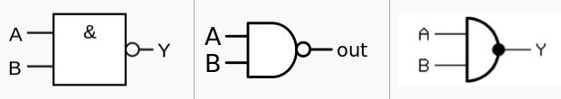
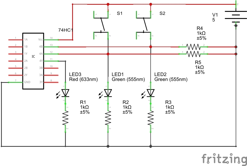
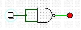
NAND symbol
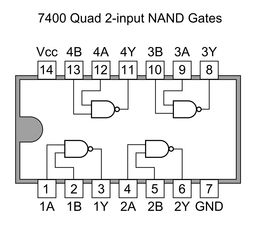
Schematic
Truth table
NAND gate
| # | 1/2/3/4 A | 1/2/3/4 B | 1/2/3/4 Y | Explanation |
|---|---|---|---|---|
| 1 | 0 | 0 | 1 | Both inputs LOW => output HIGH |
| 2 | 1 | 0 | 1 | Input A HIGH, B LOW => Output remains HIGH |
| 3 | 0 | 1 | 1 | Input A to LOW, B to HIGH => Output remains HIGH |
| 4 | 1 | 1 | 0 | Both inputs HIGH => output LOW, only LOW state |
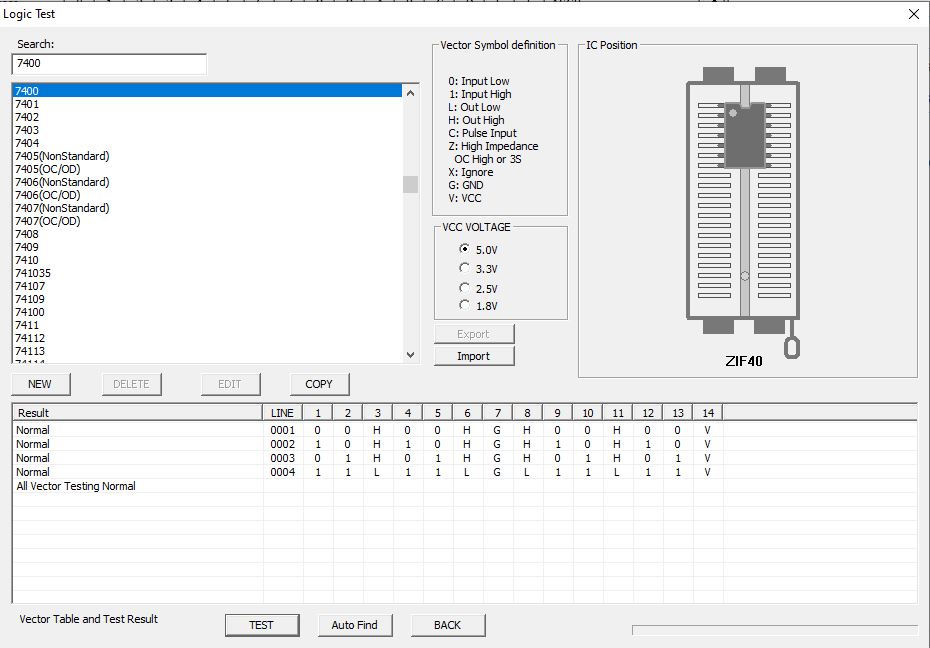
Logic tester
Data sheet
https://www.ti.com/product/de-de/SN7400
Areas of application
- Activation of ICs via bus address
- Input Control
- Logical sequences
Views
Circuit
Test
Programme
/** AND function */
bool and(bool e1, bool e2) {
    return e1 && e2;
}

/** Not a function */
bool not(bool e1){
  return !e1;
}

/** NAND-funktion */
bool nand(bool e1, bool e2){
  return not (e1 and e2);
}

void main(){
  bool output1 = nand(true, true);
  bool output2 = not(and(true, true));
  // do some output
}
Problems
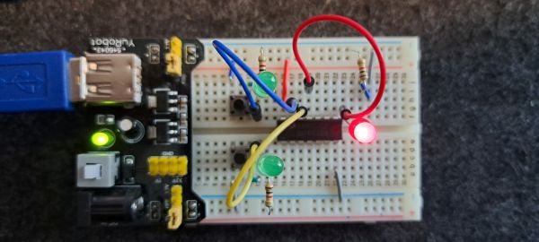
When idle, the red LED is off
Not all ICs automatically pull inputs to ground, to resolve this issue pulldown resistors must be wired between the input and ground. 1kOhm is fine, higher values are also acceptable.
Miscellaneous
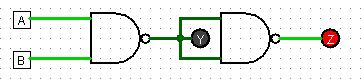
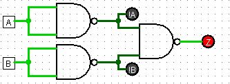
NOT circuit
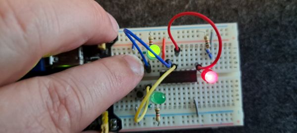
For an emergency circuit, two inputs of a NAND gate are connected. For example, pins 12 and 13 are connected; the input signal present at pin 12 is then output in inverted form at the output.
| # | Input A (12) | B (13) | Exit Z | |
|---|---|---|---|---|
| 1 | 1 | =A | 0 | Input to HIGH is inverted to output (LOW) |
| 2 | 0 | =A | 1 | The input on LOW is also inverted to the output (HIGH). |
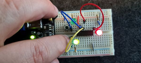
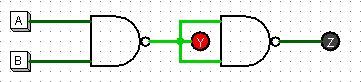
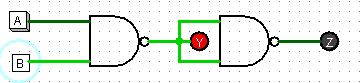
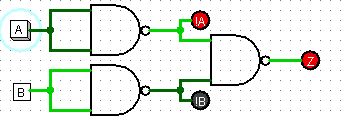
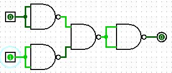
AND circuit
For the AND circuit, two gates are needed, one configured as a NAND and one as a NOT.
| # | A | B | C | D | Explanation |
|---|---|---|---|---|---|
| 1 | 0 | 0 | 1 | 0 | Both inputs on LOW, output is also LOW |
| 2 | 1 | 0 | 1 | 0 | Input A HIGH, B LOW, Output LOW |
| 3 | 0 | 1 | 1 | 0 | Input A to LOW, B to HIGH, Output LOW |
| 4 | 1 | 1 | 0 | 1 | Both inputs high, therefore the output is high |
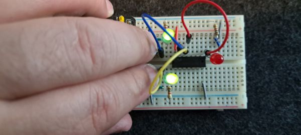
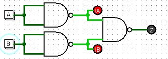
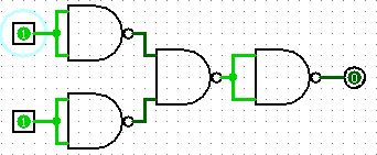
OR circuit
The OR gate requires three gates. The output is HIGH as soon as one of the inputs is set to HIGH.
| # | A | B | A | !B | Z | |
|---|---|---|---|---|---|---|
| 1 | 0 | 0 | 1 | 1 | 0 | Both inputs low, output low |
| 2 | 1 | 0 | 0 | 1 | 1 | Input A to HIGH and B to LOW, output to HIGH |
| 3 | 0 | 1 | 1 | 0 | 1 | Input A to LOW and B to HIGH, output to HIGH |
| 4 | 1 | 1 | 0 | 0 | 1 | Both inputs to HIGH, output to HIGH |
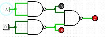
OR gate
Naturally, a NOR gate circuit is also possible. For this, another gate must be added to negate the output. If one of the inputs is HIGH, the output is always LOW.
| # | A | B | A | !B | Z | Explanation |
|---|---|---|---|---|---|---|
| 1 | 0 | 0 | 1 | 1 | 1 | Both inputs LOW, the output is HIGH |
| 2 | 1 | 0 | 0 | 1 | 0 | Input A to HIGH and B to LOW, output to LOW |
| 3 | 0 | 1 | 1 | 0 | 0 | Input A to LOW and B to HIGH, Output to LOW |
| 4 | 1 | 1 | 0 | 0 | 0 | Both inputs are HIGH, the output is LOW |
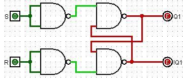
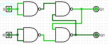
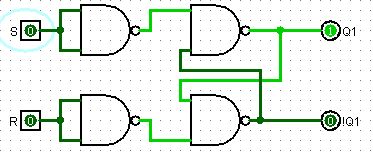
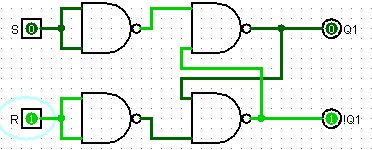
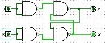
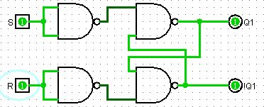
RS-FlipFlop
An RS flip-flop can also be built with the 4 gates of the 7400. The S (set) and R (reset) inputs must be negated and the outputs fed back to an input respectively. In the simulation, the outputs initially have an undefined state. In reality, it is either set or reset. The interesting thing about the RS flip-flop is that the state remains after releasing the S button and is only reset again when the R button is pressed. Thus, we can store 1 bit.
Through feedback, the preceding state must always be taken into account. For example, if Set is set to HIGH and then back to LOW, Q1 remains HIGH.
| # | S | R | !S | !R | Q1 | !Q1 | Explanation |
|---|---|---|---|---|---|---|---|
| 1 | 0 | 0 | 1 | 1 | * | * | Initial state |
| 2 | 1 | 0 | 0 | 1 | 1 | 0 | Set to HIGH |
| 3 | 0 | 0 | 1 | 1 | 1 | 0 | Set saved |
| 4 | 0 | 1 | 1 | 0 | 0 | 1 | Rest on high |
| 5 | 0 | 0 | 1 | 1 | 0 | 1 | Settings saved |
| 6 | 1 | 1 | 0 | 0 | 1 | 1 | Unacceptable condition |
| 7 | 0 | 1 | 1 | 0 | 0 | 1 | Resetz is selected |
| 8 | 0 | 0 | 1 | 1 | 0 | 1 | Reset saved |
| 9 | 1 | 1 | 0 | 0 | 1 | 1 | Unacceptable condition (2) |
| 10 | 1 | 0 | 0 | 1 | 1 | 0 | The set is chosen |
| 11 | 0 | 0 | 1 | 1 | 1 | 0 | Zustand gespeichert |
State 6, both inputs on HIGH, is impermissible. The subsequent process depends on which of the two inputs is set to LOW first. This results in the respective other one counting. If S is set to LOW first, the R input counts, meaning !Q1 is active. In the opposite case, if R is set to LOW first, the S input counts, and Q1 is active.
XNOR
The output is always HIGH when the inputs have the same potential (A=B= LOW or A=B=HIGH). This circuit requires more than just one IC.
| # | A | B | A | !B | C | D |
|---|---|---|---|---|---|---|
| 1 | 0 | 0 | 1 | 1 | 1 | 1 |
| 2 | 1 | 0 | 0 | 1 | 1 | 0 |
| 3 | 0 | 1 | 1 | 0 | 1 | 0 |
| 4 | 1 | 1 | 0 | 0 | 0 | 1 |
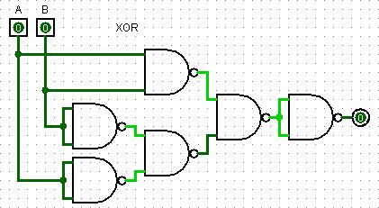
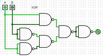
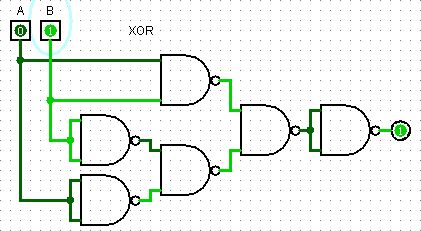
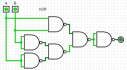
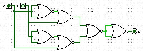
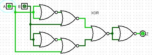
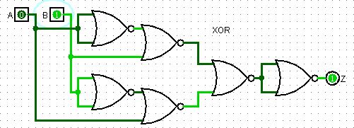
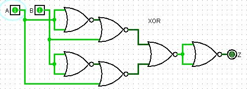
XOR
In an XOR gate, the output is HIGH when the inputs are different. This circuit requires 1.5 ICs.
| # | A | B | A | !B | C | D |
|---|---|---|---|---|---|---|
| 1 | 0 | 0 | 1 | 0 | 1 | 0 |
| 2 | 1 | 0 | 0 | 0 | 1 | 1 |
| 3 | 0 | 1 | 1 | 1 | 1 | 1 |
| 4 | 1 | 1 | 0 | 1 | 0 | 0 |
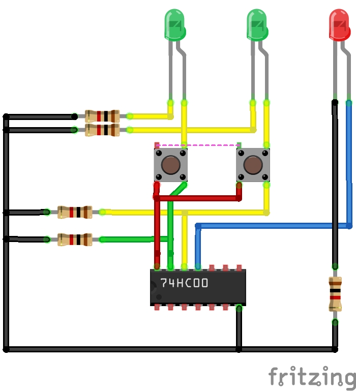
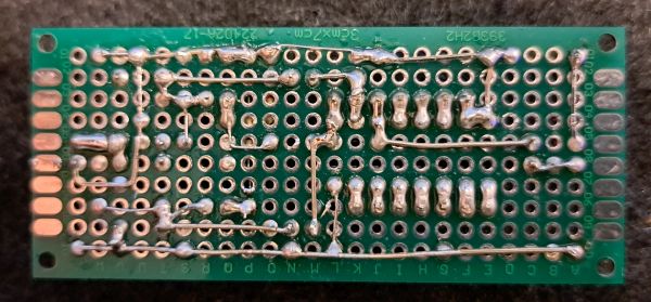
Soldered Plate
I apologise for the chaos on the circuit board, I had to retrieve skills I hadn't used for decades. The blueprint generally corresponds to the one shown above. The jumpers disconnect the LEDs and the switch from the IC to allow other circuits to be built. By the way, I am operating the circuit board with 6V (4x 1.5v AAA batteries).
I accidentally used a 16-pin IC socket. Desoldering was not an option and I didn't want to remove the bridge to ground anymore, so I simply connected pins 7 and 8 of the socket.
View
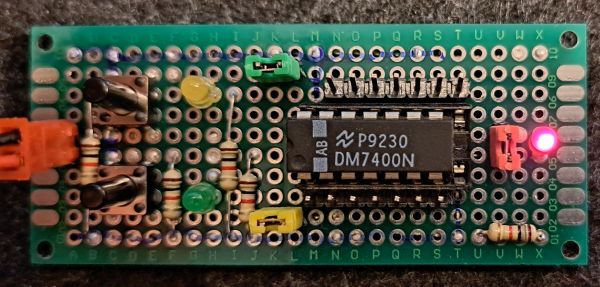
Materialliste
| Component | Number |
|---|---|
| LED Green/Yellow/Red (Can also be the same colour) | 3 |
| Jumper (Red, Green, and Yellow correspond to the selected LED colours) | 3 |
| 2 straight Polig pins | 3 |
| 2 angled pole pins for power supply | 1 |
| 7-pin plug for additional connections | 3 |
| Buttons with long press | 2 |
| 1K resistor (pulldown/pre-resistor for LED) | 5 |
| 14-pin IC socket | 1 |
| Silver wire for the connections on the back | ? |
| Solder | ? |
Addendum If you connect the LEDs in series with the pulldown resistors, you can save two resistors. The voltage of 3.5V (5V supply voltage - 1.5V LED) at the input of the IC should be sufficient to generate a HIGH.
Conclusion
A fascinating IC. Very diverse in its function. With it, by using all the gates, one can create other basic logic functions such as AND, NOR, OR, NOT, and even higher logic functions like an R/S flip-flop.
Related Posts
Sources
https://de.wikipedia.org/wiki/7400
https://www.elektronik-kompendium.de
https://sourceforge.net/projects/circuit (Logic Sim, I use it for my drawings)
Log
| Date | Description |
|---|---|
| 16.05.2024 | Entry created |
| 18.05.2024 | Pictures taken, circuit assembled and tested. |
| 24.05.2024 | Error corrected and link to TTL IC inserted. Logic circuits added. |
| 25.05.2024 | Live |
| 30.05.2024 | An RS flip-flop can be implemented using NAND gates. Board soldered. |
| 31.05.2024 | Added RS-FlipFlop and made a few marginal improvements. |
| 01.06.2024 | XOR and XNOR added. Photos of the circuit board added. |